

TaC Coated Susceptor Company Delivers Advanced CVD Susceptors for Semiconductor Manufacturing
2026-11-16
Wafer processing leaves little room for error, especially when it comes to the surfaces that hold wafers during CVD. Semicorex has stepped up with a new generation of TaC coated susceptors designed to handle the thermal stress and chemical exposure of advanced semiconductor manufacturing. The material choice alone signals a shift in how fabs approach yield and uptime. Let's unpack why.
TaC Coated Susceptors vs. Silicon Carbide: What Changes at High Temperature
At elevated temperatures, bare silicon carbide susceptors slowly degrade through surface oxidation and silicon loss, altering emissivity and creating particle contamination. A tantalum carbide coating disrupts this failure chain. TaC's melting point above 3800°C and its dense cubic lattice prevent silicon outgassing and react far less with process gases, so the susceptor surface remains dimensionally stable and chemically passive longer.
The change isn't just about lifespan. At typical MOCVD or epitaxy temperatures (1100–1600°C), uncoated SiC can form volatile SiO and CO at edges and defects, which shifts local thermal profiles and can seed defects in GaN or SiC epilayers. TaC-coated graphite or SiC susceptors hold a more uniform surface temperature because the coating's thermal conductivity and emissivity stay consistent, reducing hot spots and slip lines. Over repeated thermal cycles, the TaC layer also resists microcracking better than bulk SiC due to its higher fracture toughness at temperature.
One subtle shift shows up in wafer backside contact. Silicon carbide can react with residual oxygen to form a glassy SiO2 layer that changes contact resistance and sticks to wafers. TaC's lower oxygen affinity means the carbon is already bound in a stable carbide, so the surface stays metallic in character and releases wafers cleanly. For processes above 1500°C, this difference becomes decisive—SiC begins to lose mechanical strength, while TaC retains hardness and creep resistance.
Inside the Coating Chamber: How Uniform TaC Layers Are Applied
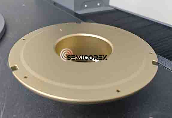
The first thing you notice inside the coating chamber is how precisely the gas flows are controlled. A blend of tantalum chloride vapor, hydrogen, and a carbon source enters through a series of preheated nozzles arranged around the substrate. The temperature is held just below the point where unwanted nucleation would occur in the gas phase — instead, the reaction is forced to happen only at the heated surface. This is what keeps the TaC layer growing evenly rather than forming loose particles that would end up as inclusions.
Rotation and tilting of the substrate play a bigger role than most people expect. The chamber isn't simply a static box; the part being coated moves continuously through a carefully mapped pattern. Each pass exposes a slightly different angle to the gas stream, which compensates for the natural tendency of corners and edges to receive more deposition than flat areas. By tuning the rotation speed against the gas flow rate, the thickness variation across a complex shape can be held to less than two microns.
What separates a truly uniform TaC layer from a mediocre one often comes down to how the pressure is pulsed during the process. Instead of holding a constant vacuum, the chamber briefly cycles between lower and higher pressure every few seconds. This momentary pressure swing changes the mean free path of the reactive species, forcing them to redistribute across the surface before the next deposition pulse begins. It's a subtle technique, but it breaks up the laminar flow pattern that would otherwise create streaking on large flat surfaces.
Why Susceptor Surface Roughness Matters More Than You Think
Most process engineers treat susceptor roughness as a secondary parameter, something to check off a spec sheet before moving on. But in epitaxial growth and CVD chambers, the surface topography of the susceptor quietly dictates how heat transfers into the wafer, how gas flows across the pocket, and whether that first monolayer nucleates evenly or scatters into defects. A mirror-smooth finish might look ideal under inspection, yet it can create micro-slip zones where the wafer shifts during ramp-up, leading to edge roll-off and thickness non-uniformity that only shows up weeks later as yield loss.
The real trouble starts when roughness changes over time. Repeated thermal cycling and exposure to process gases can etch or roughen the pocket floor, altering emissivity and local temperature gradients. A 0.2 μm Ra drift might seem trivial, but it changes how the wafer sits and how heat couples into the backside. Operators often chase ghost problems—temperature offsets, precursor depletion, even suspect thermocouples—when the root cause is a seasoned susceptor whose surface no longer matches the baseline recipe. Mapping roughness across the pocket, not just at a single point, reveals hot rings and cold centers that static metrology misses.
Rethinking roughness as an active process variable opens the door to better chamber matching and longer susceptor life. Instead of aiming for “as smooth as possible,” you can tune a specific micro-texture—directional lapping, laser dimpling, or controlled grit blasting—to stabilize wafer seating and gas boundary layers. This also reduces backside deposition, which in turn keeps roughness from drifting in the first place. The next time a film uniformity spec slips out of range, don’t rush to recalibrate the pyrometer. Flip the susceptor over and look at the surface the wafer actually touches.
Thermal Cycling Stress and How TaC Extends Service Intervals
Repeated heating and cooling cycles are brutal on high-temperature components. Each swing forces the material to expand and contract, but different phases or adjacent regions rarely move at the same rate. This mismatch builds localized stress at grain boundaries, coating interfaces, and sharp corners. Over hundreds or thousands of cycles, tiny cracks start to open up. They don't need a single catastrophic event to spread—just the steady accumulation of micro-damage that eventually links into a network and causes spalling, delamination, or outright fracture.
Tantalum carbide changes that failure timeline. Its lattice stays stable across an unusually wide temperature range, so it doesn't undergo the sudden volume shifts that plague many other hard ceramics. The strong Ta-C bonds resist dislocation motion and crack nucleation even when the surrounding metal or substrate is straining. As a result, a TaC-containing layer can absorb the mismatch stresses without tearing itself apart. Instead of cracks propagating after a few dozen thermal cycles, the coating holds together, keeping the underlying part protected much longer.
In practical terms, that means equipment can stay online through more start-stop sequences and rapid load changes before maintenance is required. Fewer forced outages, fewer teardowns for crack inspection, and longer stretches between part replacements all trace back to that fundamental resistance to thermal cycling damage.
Real-World Throughput Gains from Longer-Lasting Susceptors
Conventional susceptor films in industrial microwave tunnels degrade after a few hundred heating cycles. The metallized layer starts to crack, resistance climbs unevenly, and hot spots appear. Operators respond by slowing the belt or replacing the film every shift, which directly eats into line throughput. A susceptor that survives 3,000 cycles without measurable drift removes that forced downtime altogether.
In a ready-meal packaging line, switching to a ceramic-reinforced susceptor extended replacement intervals from every 4 hours to once every 9 days. The line ran 11% more product per shift simply because it no longer stopped for film changes. No changes to power settings or conveyor speed were needed—the gain came purely from eliminating scheduled and unscheduled interruptions tied to susceptor failure.
The throughput effect compounds when multiple microwave tunnels share a single packing area. If each tunnel avoids two 15-minute stoppages per day, a four-tunnel facility recovers two hours of production daily. Maintenance crews also shift from reactive film swaps to planned inspections, further stabilizing output. Longer-lasting susceptors turn a consumable into a near-fixed asset, and the line speed no longer has to compensate for degrading heating performance.
Evaluating a TaC Coated Susceptor Partner for Advanced Nodes
Selecting a susceptor partner for advanced node processing demands a close look at how the TaC coating behaves under real deposition conditions. The coating’s thermal stability and resistance to halogen-based etch chemistries are table stakes, but what separates a workable partner is their control over the coating’s microstructure. Voids, micro-cracks, or uneven grain boundaries near the wafer pocket can shift local temperature profiles, causing film thickness drift across the wafer. A partner that routinely shares cross-sectional SEM or XRD data from each coating lot, rather than only providing a generic datasheet, is far more valuable when you’re trying to lock down a stable process window for sub-5nm features.
Beyond the material itself, the evaluation needs to probe how the partner handles thermal cycling and pre-coat conditioning. Advanced nodes often push susceptor temperatures above 700°C, and repeated ramp-up/cool-down cycles can delaminate poorly bonded TaC layers. Ask for thermal shock test results that mimic your specific chamber recipe, not just steady-state exposure data. Another overlooked area is surface roughness evolution: as wafers are loaded and unloaded, abrasive contact can wear down the TaC coating, exposing the underlying graphite and releasing particles. A partner that tracks roughness changes over hundreds of simulated wafer transfers, with before-and-after AFM scans, gives you confidence that particle performance won’t degrade mid-production.
Finally, look at the partner’s ability to tune the coating for your specific process gases and precursors. TaC coatings are not one-size-fits-all; the carbon-to-tantalum ratio, doping with trace elements, and post-coat annealing all shift the surface reactivity. A strong partner will run a design-of-experiments with your gas mix, measuring not just etch rate but also byproduct formation and wafer backside contamination. Responsiveness matters here: if they can iterate on coating parameters within a few weeks and provide transparent metrology data—like SIMS depth profiles for metal contamination—then you have a partner who can keep pace with the rapid changes typical of advanced node development.
FAQ
TaC creates a dense, chemically inert surface that resists attack from chlorine and hydrogen radicals at temperatures above 1500°C. This keeps the susceptor from degrading, reduces particle generation, and extends the interval between maintenance cycles.
The coating is applied with a graded interface that bonds tightly to the graphite base, allowing the susceptor to endure repeated thermal shocks without spalling. We also match the coefficient of thermal expansion between layers to minimize micro-cracking.
Almost every dimension and feature can be adapted. We adjust pocket depth, edge lip geometry, overall diameter, and coating thickness to suit different wafer sizes and gas flow patterns. Special purge holes or backside textures are also possible.
The main yield gains come from lower metal contamination and fewer slip lines. TaC prevents graphite particles from shedding onto wafers and maintains a flat, stable surface for uniform temperature distribution, which reduces warpage and crystal defects.
Yes, we offer a full refurbishment service. We strip the old coating, inspect the graphite for damage, machine the surface if needed, and apply a fresh TaC layer. Many fabs save 40-60% compared to buying new susceptors.
Each susceptor goes through ultrasonic scanning for bond integrity, X-ray fluorescence for coating thickness, and a thermal cycling test up to 1600°C. We also inspect surface roughness with laser profilometry and provide a full dimensional report.
They are widely used in silicon carbide epitaxy, gallium nitride MOCVD, and silicon germanium deposition. Power electronics and RF device makers see the biggest impact because those processes run hot and use aggressive precursors that quickly degrade standard graphite.
Conclusion
As wafer processing shifts to higher temperatures and aggressive precursor chemistries, silicon carbide susceptors often show their limits through micro-cracking, particle shedding, and unstable resistivity drift. A switch to TaC-coated susceptors changes that picture. The tantalum carbide layer resists carburization and maintains a dense, low-roughness face under repeated thermal cycles, which cuts down on both contamination and the need for frequent chamber wet cleans. Because the TaC is applied through a controlled CVD process, thickness stays uniform even across deep pockets and edge steps, so wafer temperature profiles remain tighter and film deposition stays consistent from run to run.
That consistency translates directly into throughput. Instead of swapping susceptors every few hundred cycles, fabs running advanced nodes report longer service intervals and measurable gains in available chamber hours. The reduced surface degeneration also helps with particle performance, which matters more as device geometries shrink. When evaluating a supplier, it is worth asking about coating adhesion after thermal shock, demonstrated roughness data, and how the TaC layer behaves with your specific process gases. A partner that can show long-run data from high-volume tools, not just coupon tests, is the one likely to help you extend preventive maintenance windows without risking wafer yield.
Contact Us
Contact Person: Svenja Wei
Email: [email protected]
Tel/WhatsApp: +8613567891907
Website: https://www.semicorex.com